Silicon wafers are thin slices of silicon. They are used to make integrated circuits and microdevices. These wafers are vital for our everyday technology.
These wafers can come in different forms, but one of the most exciting and advanced types is the patterned silicon wafer. What are they, and why are they so important? Let’s dive into the fascinating world of silicon wafers!
What Are Silicon Wafers?
Silicon wafers are thin, circular discs carefully crafted from a single crystal of silicon. Typically ranging from a few millimeters to several inches in diameter, they serve as the foundation or substrate for a wide range of electronic devices, from simple microchips to complex semiconductor components.
To illustrate their significance, imagine a blank canvas waiting to be painted – a pristine slate ready to be transformed by the ingenuity of engineers and scientists. Just as an artist brings a canvas to life with colors and shapes, these experts use silicon wafers as a base to design, prototype, and manufacture innovative electronic systems.
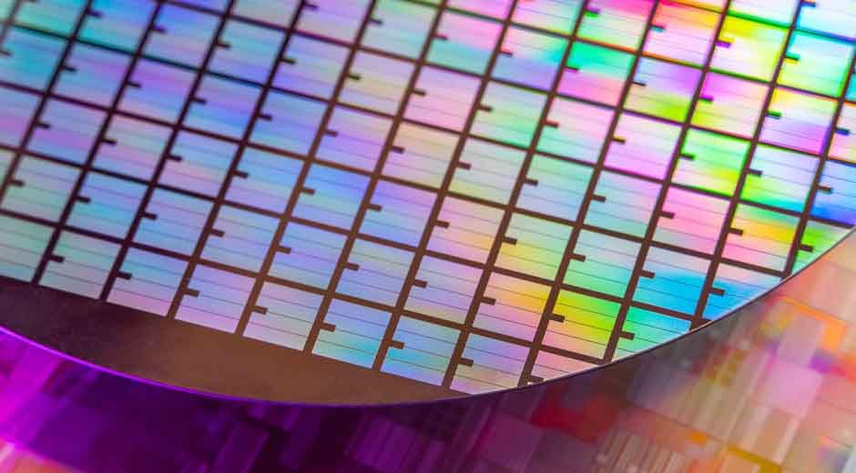
The Importance of Patterned Silicon Wafers
Patterned silicon wafers are specially designed with intricate patterns on their surface. These patterns help in the manufacturing of various components, including chips, sensors, and photonics devices. By using patterned silicon wafers, manufacturers can create much more complex and functional devices than they could with plain wafers.
These wafers play a significant role in developing technology, making devices smaller, faster, and more efficient. They are essential in everything from smartphones to computers and even in medical devices.
Applications of Patterned Silicon Wafers
Patterned silicon wafers, with their unique surface structures, have far-reaching implications in various industries, revolutionizing the way we approach innovation. Here are some key areas where their impact is most significant:
Electronics
The modern gadgets we can’t live without, like smartphones, laptops, and tablets, owe their existence to patterned silicon wafers. These wafers help make tiny integrated circuits. These circuits act as the brains of our devices. They process information and perform tasks really fast.
For instance, the smartphone you’re holding right now relies on a complex network of these circuits to connect you to the world. Without patterned silicon wafers, our devices would be much larger, slower, and less powerful.
Sensors
Patterned silicon wafers also play a crucial role in sensors, which enable devices to perceive and respond to their surroundings. For example, car pressure sensors can spot tiny changes in air pressure. This helps keep tire pressure just right and boosts road safety.
Similarly, temperature sensors in smartphones can detect even the slightest increase in device temperature, preventing overheating and ensuring smooth performance. These sensors are made possible by the precision and miniaturization enabled by patterned silicon wafers.
Photonics
Photonics, the science of light, relies heavily on patterned silicon wafers to create innovative devices that transform the way we communicate and entertain. Lasers, for instance, are made possible by these wafers, which allow for the precise control of light waves.
This technology is used in everything from high-speed data transmission to medical treatments. LED lights, another photonics breakthrough, are also made possible by patterned silicon wafers. These energy-efficient lights illuminate our homes, power our devices, and light up our streets, contributing to a brighter, more sustainable future.
How Are Patterned Silicon Wafers Made?
Creating patterned silicon wafers is a intricate and meticulous process that involves several precise steps. It begins with a silicon ingot, a large crystal rod grown in a controlled environment to minimize impurities.
Creating patterned silicon wafers is a complex process that includes several steps:
Growing the Silicon
The journey to create microchips begins with cultivating a massive, perfect crystal of silicon. This is often achieved through the Czochralski process, a technique pioneered by Polish scientist Jan Czochralski in 1918. In this process, a small seed crystal is dipped into a vat of molten silicon, and then slowly pulled upwards while rotating.
As it rises, the molten silicon solidifies onto the seed, forming a single crystal ingot. This ingot is then carefully extracted from the vat, and its purity is inspected to ensure it meets the ultra-high standards required for microchip production.
Cutting the Wafers
Once the crystal ingot has been grown, it’s sliced into thin, delicate wafers using a precision diamond saw. The saw blade, typically coated with diamond dust, is designed to make precise cuts without damaging the silicon. The wafers are then polished to remove any imperfections, producing a smooth, flat surface for the next stages of production.
Patterning
The most critical step in microchip creation is adding patterns to the wafers. This intricate process, known as patterning, can be achieved through various methods, including photolithography.
Photolithography involves coating the wafer with a light-sensitive photoresist layer, which is then exposed to ultraviolet light through a patterned mask. The areas of the photoresist layer that are exposed to light undergo a chemical change, allowing the desired patterns to be transferred onto the wafer.
Etching
After developing the photoresist, the exposed areas of silicon are chemically etched away, creating the intricate patterns and structures necessary for the microchip’s electronic pathways.
The etching process involves bathing the wafer in a series of chemicals, which selectively remove the silicon in the exposed areas. The resulting patterns are then inspected to ensure their accuracy and precision, as even the slightest deviation can render the microchip useless.
The Future of Patterned Silicon Wafers
The future of patterned silicon wafers looks promising as technology continues to advance. Researchers are constantly exploring new ways to use them for even more innovative applications. Future developments could include enhanced devices that are lighter, faster, and consume less energy.
Moreover, as the demand for renewable energy grows, patterned silicon wafers are also being explored for solar panel production, making them vital in the fight against climate change.
The Vital Role of Silicon Wafers
Silicon wafers, particularly patterned silicon wafers, are essential in shaping our technological landscape. Their applications in electronics, sensors, and photonics drive innovation and progress in modern technology. As we look toward the future, these wafers will become even more crucial in creating smarter, more efficient devices.
To learn more about the significance of these devices, consider checking resources related to patterned silicon wafers.